electron microscope
Types of Electron Microscope

Electron microscope is used to study and observe cells, molecules, micro-organisms, crystals, metals and a number of other organic and inorganic specimens. Most modern electron microscopes can magnify the specimen up to 2 million times. The quality of the image, resolution, etc., however, depend greatly on the type of the electron microscope used.
Electron microscope can be divided into five types:
Transmission electron microscope (TEM)
It is the earliest form of electron microscope. It works on the same principles as the traditional light microscopes with the difference that it uses a beam of electrons under high voltage instead of light. The electrons which are transmitted (therefore transmission electron microscope) through the sample create a magnified image on an imaging device which can be a fluorescent screen, photographic film or a CCD camera. The TEM produces black and white two-dimensional image of the specimen, however, it is also possible to get a three-dimensional representation of the material by the use of the so-called ptychography that was invented by Walter Hoppe and Fourier-based back projection.
Scanning electron microscope (SEM)
The scanning electron microscope (SEM) uses high voltage electron beam as well but in contrary to the TEM, the SEM focuses the beam of electrons on a narrow spot and creates image by scanning the specimen in a raster (therefore scanned electron microscope). Although the first prototype of the SEM was developed as early as 1937, this electron microscope became useful only after it was improved by Sir Charles Oatley in the 1960s. Its main advantage over the TEM is the ability to image specimens which are wet or in a low vacuum, while the fact that it relies on the surface scanning rather than transmission of electron beam through the sample, has made imagining of organic samples a lot easier. The type of SEM which is used for imaging wet and low vacuum specimens is known as environmental scanning electron microscope (ESEM). Both the standard SEM and ESEM produce a high quality three-dimensional image of the specimen.
Reflection electron microscope (REM)
This type of electron microscope uses scattered electrons that reflect from the surface of the specimen to produce an image. It works similar to the SEM but instead of using the secondary electrons, the REM uses elastically scattered electrons to create an image. It involves the used of a technique known as the reflection high-energy electron diffraction (RHEED) or reflection high-energy loss spectroscopy (RHELS).
Scanning transmission electron microscope (STEM)
Widely considered a high resolution version of the SEM, the scanning transmission electron microscope (STEM) focuses on a narrow spot and produces image by scanning the sample in a raster. However, it also “picks up” the electrons which go through the specimen and produces a resolution comparable to the TEM by using the SEM technique.
Low-voltage electron microscope (LVEM)
The low-voltage electron microscope (LVEM) is a unique blend of the TEM, SEM and STEM. Like its name suggests, it uses low-voltage which makes it especially useful for imaging of biological and organic specimens.

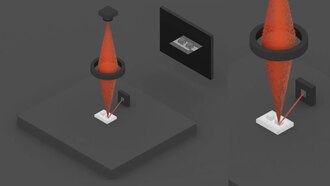
Types of Electron Microscopes
There are several different types of electron microscopes, including the transmission electron microscope (TEM), scanning electron microscope (SEM), and reflection electron microscope (REM.) Each of these types of the electron microscope will be described in more detail in this article, including the benefits and disadvantages of each.
Transmission electron microscope (TEM)
The transmission electron microscope is the original type of electron microscope, which directs a high voltage electron beam towards the specimen to illuminate it and create a magnified image of the sample.

The image shows the cross section of a capillary with a red blood cell present, taken using a transmission electron microscpe.
An electron gun is used to produce the electron beam. The gun is usually fitted with a tungsten filament cathode, which is the source of the electron beam. An anode is used to accelerate the electron beam, and electrostatic and electromagnetic lenses help to focus the beam.
When the electron beam passes through the specimen, it is scattered and provides an image of the microscopic structure of the specimen, which can be viewed through the objective lens of the microscope.
The spatial variation can be examined by projecting the image onto a fluorescent zinc sulfide coated screen. Another method that can be used to record the image is to place a photographic film into the electron beam, which will record the image. A digital camera can also be used to display the image on a computer screen in real time.
Spherical aberration has traditionally limited the resolution of transmission electron microscopes. However, recent developments have helped to overcome this issue to increase resolution with hardware correction of the spherical aberration. As a result, it is now possible to produce images with a resolution below 0.5 angstrom and more than 50 million times magnifications.
The most significant limitation of the transmission microscope is the requirement for very thin specimen samples, usually less than 100 nm. As a result, most biological specimens need to be chemically fixed and dehydrated, in order to be embedded in a polymer resin so that it can be viewed with a TEM.
Scanning electron microscope (SEM)
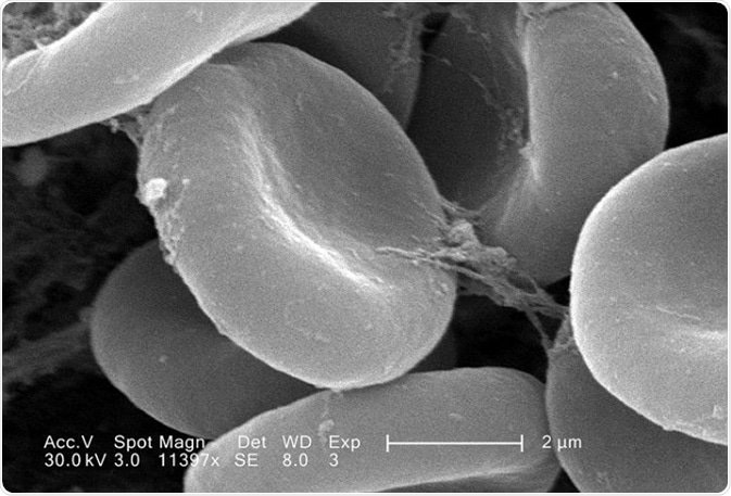
The scanning electron microscope used a technique known as raster scanning to produce magnified images of the specimen. It directs a focused electron beam across the rectangular area of the specimen, which loses energy as it passes through. The energy is converted into other forms of energy, such as heat, light, secondary electrons, and backscattered electrons. This information can be translated to view the topography and composition of the original specimen.

The image shows red blood cells, taken using a scanning electron microscpe.
The resolution of scanning electron microscopes tends to be poorer than that achieved with a transmission electron microscope.
However, it is beneficial because it utilizes surface processes and can hence create images of large samples, up to several centimeters in size, and has a greater depth of field. As a result, the images from an SEM can be good representations of the real shape of the specimen.
Additionally, a specific type of SEM known as environmental scanning electron microscope (ESEM) is able to image samples that are wet or contained in gas. This increases the range of possibilities for which the microscope can be used.
Reflection electron microscope (REM)
The reflection electron microscope involves the detection of a beam of elastically scattered electrons that is reflected off of the specimen that is being examined. The reflection high-energy electron diffraction (RHEED) and reflection high-energy loss spectroscopy (RHELS) techniques are often used in this type of microscopy.
Types[edit]
Transmission electron microscope (TEM)[edit]
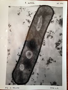
The original form of the electron microscope, the transmission electron microscope (TEM), uses a high voltage electron beamto illuminate the specimen and create an image. The electron beam is produced by an electron gun, commonly fitted with a tungsten filament cathode as the electron source. The electron beam is accelerated by an anode typically at +100 keV (40 to 400 keV) with respect to the cathode, focused by electrostatic and electromagnetic lenses, and transmitted through the specimen that is in part transparent to electrons and in part scatters them out of the beam. When it emerges from the specimen, the electron beam carries information about the structure of the specimen that is magnified by the objective lenssystem of the microscope. The spatial variation in this information (the "image") may be viewed by projecting the magnified electron image onto a fluorescent viewing screen coated with a phosphor or scintillator material such as zinc sulfide. Alternatively, the image can be photographically recorded by exposing a photographic film or plate directly to the electron beam, or a high-resolution phosphor may be coupled by means of a lens optical system or a fibre optic light-guide to the sensor of a digital camera. The image detected by the digital camera may be displayed on a monitor or computer.
The resolution of TEMs is limited primarily by spherical aberration, but a new generation of hardware correctors can reduce spherical aberration to increase the resolution in high-resolution transmission electron microscopy (HRTEM) to below 0.5 angstrom (50 picometres),[1] enabling magnifications above 50 million times.[10] The ability of HRTEM to determine the positions of atoms within materials is useful for nano-technologies research and development.[11]
Transmission electron microscopes are often used in electron diffraction mode. The advantages of electron diffraction over X-ray crystallography are that the specimen need not be a single crystal or even a polycrystalline powder, and also that the Fourier transform reconstruction of the object's magnified structure occurs physically and thus avoids the need for solving the phase problem faced by the X-ray crystallographers after obtaining their X-ray diffraction patterns of a single crystal or polycrystalline powder.
One major disadvantage of the transmission electron microscope is the need for extremely thin sections of the specimens, typically about 100 nanometers. Creating these thin sections for biological and materials specimens is technically very challenging. Semiconductor thin sections can be made using a focused ion beam. Biological tissue specimens are chemically fixed, dehydrated and embedded in a polymer resin to stabilize them sufficiently to allow ultrathin sectioning. Sections of biological specimens, organic polymers, and similar materials may require staining with heavy atom labels in order to achieve the required image contrast.
Serial-section electron microscopy (ssEM)[edit]
One application of TEM is serial-section electron microscopy (ssEM), for example in analyzing the connectivity in volumetric samples of brain tissue by imaging many thin sections in sequence.[12]
Scanning electron microscope (SEM)[edit]
The SEM produces images by probing the specimen with a focused electron beam that is scanned across a rectangular area of the specimen (raster scanning). When the electron beam interacts with the specimen, it loses energy by a variety of mechanisms. The lost energy is converted into alternative forms such as heat, emission of low-energy secondary electronsand high-energy backscattered electrons, light emission (cathodoluminescence) or X-ray emission, all of which provide signals carrying information about the properties of the specimen surface, such as its topography and composition. The image displayed by an SEM maps the varying intensity of any of these signals into the image in a position corresponding to the position of the beam on the specimen when the signal was generated. In the SEM image of an ant shown below and to the right, the image was constructed from signals produced by a secondary electron detector, the normal or conventional imaging mode in most SEMs.
Generally, the image resolution of an SEM is lower than that of a TEM. However, because the SEM images the surface of a sample rather than its interior, the electrons do not have to travel through the sample. This reduces the need for extensive sample preparation to thin the specimen to electron transparency. The SEM is able to image bulk samples that can fit on its stage and still be maneuvered, including a height less than the working distance being used, often 4 millimeters for high-resolution images. The SEM also has a great depth of field, and so can produce images that are good representations of the three-dimensional surface shape of the sample. Another advantage of SEMs comes with environmental scanning electron microscopes (ESEM) that can produce images of good quality and resolution with hydrated samples or in low, rather than high, vacuum or under chamber gases. This facilitates imaging unfixed biological samples that are unstable in the high vacuum of conventional electron microscopes.
Color[edit]
In their most common configurations, electron microscopes produce images with a single brightness value per pixel, with the results usually rendered in grayscale.[13] However, often these images are then colorized through the use of feature-detection software, or simply by hand-editing using a graphics editor. This may be done to clarify structure or for aesthetic effect and generally does not add new information about the specimen.[14]
In some configurations information about several specimen properties is gathered per pixel, usually by the use of multiple detectors.[15] In SEM, the attributes of topography and material contrast can be obtained by a pair of backscattered electron detectors and such attributes can be superimposed in a single color image by assigning a different primary color to each attribute.[16] Similarly, a combination of backscattered and secondary electron signals can be assigned to different colors and superimposed on a single color micrograph displaying simultaneously the properties of the specimen.[17]
Some types of detectors used in SEM have analytical capabilities, and can provide several items of data at each pixel. Examples are the Energy-dispersive X-ray spectroscopy (EDS) detectors used in elemental analysis and Cathodoluminescence microscope (CL) systems that analyse the intensity and spectrum of electron-induced luminescence in (for example) geological specimens. In SEM systems using these detectors, it is common to color code the signals and superimpose them in a single color image, so that differences in the distribution of the various components of the specimen can be seen clearly and compared. Optionally, the standard secondary electron image can be merged with the one or more compositional channels, so that the specimen's structure and composition can be compared. Such images can be made while maintaining the full integrity of the original signal, which is not modified in any way.
Reflection electron microscope (REM)[edit]
In the reflection electron microscope (REM) as in the TEM, an electron beam is incident on a surface but instead of using the transmission (TEM) or secondary electrons (SEM), the reflected beam of elastically scattered electrons is detected. This technique is typically coupled with reflection high energy electron diffraction (RHEED) and reflection high-energy loss spectroscopy (RHELS).[citation needed] Another variation is spin-polarized low-energy electron microscopy (SPLEEM), which is used for looking at the microstructure of magnetic domains.[18]
Scanning transmission electron microscope (STEM)[edit]
The STEM rasters a focused incident probe across a specimen that (as with the TEM) has been thinned to facilitate detection of electrons scattered through the specimen. The high resolution of the TEM is thus possible in STEM. The focusing action (and aberrations) occur before the electrons hit the specimen in the STEM, but afterward in the TEM. The STEMs use of SEM-like beam rastering simplifies annular dark-field imaging, and other analytical techniques, but also means that image data is acquired in serial rather than in parallel fashion. Often TEM can be equipped with the scanning option and then it can function both as TEM and STEM.
. A focused ion beam (FIB) instrument is almost identical to a SEM, but uses a beam of ions rather than electrons. The focused ion beam can directly modify or "mill" the specimen surface, via the sputtering process, and this milling can be controlled with nanometer precision. By carefully controlling the energy and intensity of the ion beam, it is possible to perform very precise nano-machining to produce minute components or to remove unwanted material. In addition, ion beam assisted chemical vapor deposition can be used to deposit material with a level of precision similar to FIB milling. A small quantity of a specifically selected precursor gas is injected into the vicinity of the beam, where it is decomposed by the beam, depositing the nonvolatile decomposition products on the specimen surface while the volatile products are extracted by the vacuum system.
A FIB becomes even more powerful when it is combined with a SEM as in the Thermo Scientific DualBeam system. In a DualBeam, the electron and ion beams intersect at a 52° angle at a coincident point near the sample surface, allowing immediate, high resolution SEM imaging of the FIB-milled surface. Such systems combine the benefits of both the SEM and FIB and provide complementary imaging and beam chemistry capabilities.
A scanning electron microscope (SEM), like a transmission electron microscope, consists of an electron optical column, a vacuum system, electronics, and software. The column is considerably shorter because the only lenses needed are those above the specimen used to focus the electrons into a fine spot on the specimen surface. The specimen chamber, however, is larger because the SEM technique does not impose any restriction on specimen size other than chamber size.
The electron gun at the top of the column produces an electron beam that is focused into a fine spot as small as 1 nm in diameter on the specimen surface. This beam is scanned in a rectangular raster over the specimen and the intensities of various signals created by interactions between the beam electrons and the specimen are measured and stored in computer memory. The stored values are then mapped as variations in brightness on the image display. The secondary electron (SE) signal is the most frequently used signal. It varies with the topography of the sample surface much like an aerial photograph: edges are bright, recesses are dark. The ratio of the size of the displayed image to the size of the area scanned on the specimen gives the magnification.
Aberration-corrected transmission electron microscopy
The recent development of a dedicated commercial aberration-corrected TEM has enabled major advances in TEM capability. Without correction,TEM resolution is limited primarily by spherical aberration, resulting in a general blurring of the image, but also in a phenomenon called delocalization, in which periodic structures appear to extend beyond their actual physical boundaries. The ability to correct spherical aberration leaves the reduction or correction of the effects of chromatic aberration as the next major challenge in improving TEM performance. Chromatic aberration correctors have been successfully incorporated into the Thermo Scientific™ Titan™ TEM platform, but their design and operation are substantially more complex than spherical aberration correctors.
Environmental transmission electron microscopy
An environmental TEM (ETEM), such as Thermo Scientific™ Titan ETEM, uses a specially designed vacuum system to allow researchers to observe specimens in a range of conditions approaching more "natural" environments, with gas pressures in the sample chamber as high as a few percent of atmospheric pressure. This is important for observing interactions between the sample and the environment. ETEM relies on pressure-limiting apertures and differential vacuum pumping to permit less restrictive vacuum conditions in the vicinity of the sample while maintaining high vacuum in the rest of the electron column.




Comments
Post a Comment